Key Engineering Takeaways
- •A transistor is a 3-terminal semiconductor device that uses a tiny input signal to control a much larger output current.
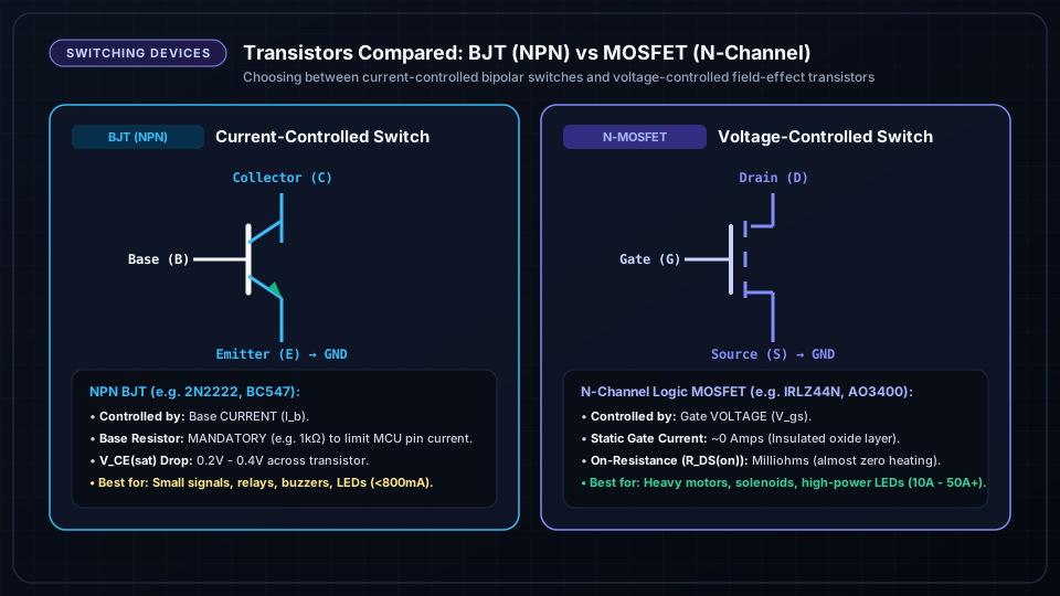
- •BJTs are CURRENT-CONTROLLED (Base current Ib controls Collector current Ic: Ic = β · Ib).
- •MOSFETs are VOLTAGE-CONTROLLED (Gate voltage Vgs controls Drain current Id with near-zero gate input current).
- •In Cutoff mode, the transistor is an open switch (OFF); in Saturation mode, it is a closed switch (ON) with minimal voltage drop.
- •For high-power robotics motor drivers (>2A), use logic-level N-Channel MOSFETs (IRLZ44N) instead of BJTs to prevent overheating.
- • Ohm's law and Diode PN junctions
- • 2N2222 / BC547 NPN Transistor
- • IRLZ44N Logic-Level N-MOSFET
- • 1kΩ Resistor
- • 12V DC Motor / Relay
- • Flyback Diode (1N4007)
What is a Transistor? The Electronic Switch & Amplifier
Invented at Bell Labs in 1947 by Bardeen, Brattain, and Shockley, the Transistor is the most important invention of the modern technological era.
Microcontrollers (like an ESP32 or Raspberry Pi) can only output tiny currents (typically 10mA - 20mA at 3.3V). Attempting to connect a 12V high-torque robot motor or relay directly to a GPIO pin will instantly destroy the microcontroller.
A transistor bridges this gap by acting as an electronic relay: a tiny 5mA signal from your microcontroller turns on a massive 10A motor current without any moving mechanical parts!
Bipolar Junction Transistors (BJT): NPN vs PNP Working
A Bipolar Junction Transistor (BJT) consists of three layered semiconductor regions:
Terminals:
- Base (B): The control terminal (like a valve handle).
- Collector (C): High-voltage/current enters here (in NPN).
- Emitter (E): Current exits here to ground.
NPN vs PNP:
- NPN Transistor: Turns ON when Base is HIGH (V_B > 0.7V relative to Emitter). Current flows from Collector to Emitter. Most commonly used for low-side switching.
- PNP Transistor: Turns ON when Base is pulled LOW (V_B < V_E - 0.7V). Used for high-side switching.
Using an NPN BJT (2N2222 / BC547) as a Digital Switch
To use an NPN transistor as a clean ON/OFF switch:
- 1Connect Emitter to Ground (0V).
- 2Connect your load (e.g. Relay coil or 12V LED strip) between the +12V Power Supply and the Collector.
- 3Connect the microcontroller GPIO pin through a 1 kΩ Base Resistor to the Base.
When GPIO output is 0V (LOW) to No base current to Transistor is in Cutoff (OFF). When GPIO output is 3.3V (HIGH) to Base current flows to Transistor enters Saturation (ON), pulling Collector to 0.2V and powering the load.
MOSFETs: Voltage-Controlled High-Current Switching
For heavy loads (>1 Ampere), MOSFETs (Metal-Oxide-Semiconductor Field-Effect Transistors) are superior to BJTs.
Terminals:
- Gate (G): Isolated by a glass-like silicon dioxide insulator. Zero DC current flows into the Gate!
- Drain (D): Connects to the load.
- Source (S): Connects to ground (for N-Channel).
When voltage applied to the Gate exceeds the threshold voltage (V_GS(th)), an electric field opens an electron channel between Drain and Source with ultra-low internal resistance (R_DS(on) < 0.02 Ω), allowing dozens of Amperes without heat.
Frequently Asked Questions
Why do I need a base resistor on a BJT but not on a MOSFET?
A BJT Base-Emitter junction is physically a forward-biased diode. Without a Base current-limiting resistor, excessive current will rush in from the microcontroller pin and burn out both the pin and the transistor. A MOSFET gate is an open insulator, though a small 100Ω gate resistor is used to dampen high-frequency ringing.
What is a Logic-Level MOSFET?
Standard power MOSFETs require 10V on the Gate to fully turn ON. A Logic-Level MOSFET (such as IRLZ44N or AO3400) is engineered to fully saturate with just 3.3V to 5V on the Gate, making them directly compatible with microcontrollers.