Key Engineering Takeaways
- •A diode allows electric current to flow in ONE direction only (Anode to Cathode) and blocks current in reverse.
- •Silicon diodes require approximately 0.7V forward threshold voltage (0.3V for Schottky) before they begin conducting.
- •The silver/white painted stripe on a physical diode marks the CATHODE (Negative terminal).
- •LEDs emit light when electrons recombine with holes in the PN junction, requiring an external series resistor to prevent burnout.
- •Flyback diodes placed across inductive motor coils eliminate dangerous 100V+ voltage spikes when motors turn off.
- • Basic Voltage and Current
- • 1N4007 Silicon Diodes
- • Assorted LEDs (Red, Green, Blue)
- • 1N4148 Fast Switching Diode
- • Breadboard
What is a Diode? The Electrical One-Way Valve
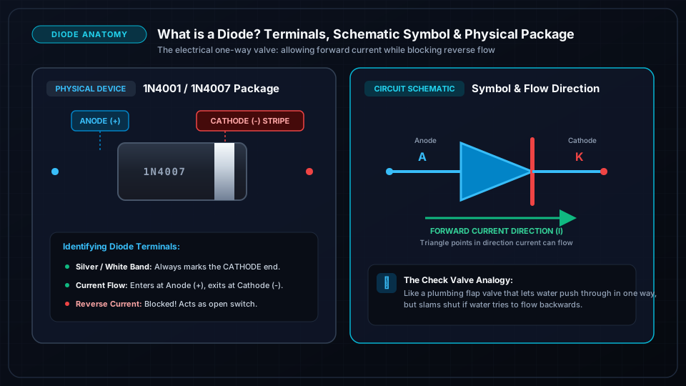
A Diode is a specialized two-terminal semiconductor device that acts as a one-way check valve for electric current.
It allows current to flow freely in one direction (Forward Bias), while providing virtually infinite resistance to current attempting to flow in the reverse direction (Reverse Bias).
Diode Terminals:
- Anode (A, Positive terminal): Current enters here.
- Cathode (K, Negative terminal): Current exits here.
- On standard physical cylindrical diodes (like the 1N4001/1N4007), a silver or white ring band marks the Cathode end.
The PN Junction: Forward Bias vs Reverse Bias
Diodes are manufactured by joining P-type silicon (rich in positive charge holes) with N-type silicon (rich in free electrons), forming a PN Junction:
1. Forward Bias (Conducting):
When the positive battery terminal connects to the Anode (P) and negative to Cathode (N), external voltage overcomes the internal barrier potential (0.7V for Silicon, 0.3V for Schottky). The depletion zone shrinks and heavy current conducts with a constant 0.7V drop across the diode.
2. Reverse Bias (Blocking):
When positive connects to Cathode (N) and negative to Anode (P), electrons and holes are pulled away from the junction, widening the depletion barrier. Current is blocked completely (leakage is negligible, <1µA).

Light Emitting Diodes (LEDs) & Sizing Resistors
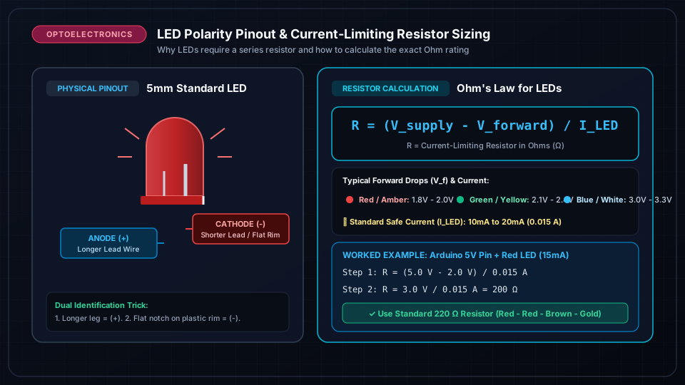
A Light Emitting Diode (LED) is a specialized diode designed to release photon energy (light) when electrons fall across its bandgap.
Unlike incandescent light bulbs, LEDs have zero internal resistance once conducting. Connecting an LED directly to a 5V battery will cause infinite current flow and instantly vaporize the silicon die!
LED Current-Limiting Resistor Formula:
Typical Forward Voltage Drops (V_f) by Color:
- Red / Amber: 1.8V - 2.0V
- Green / Yellow: 2.1V - 2.4V
- Blue / White: 3.0V - 3.3V
- Target Current (I_LED): Typically 10mA to 20mA (0.015A).
Example: Sizing a resistor for a Red LED (V_f = 2.0V) on a 5V Arduino pin at 15mA:
Full-Wave Bridge Rectifier: Turning AC into DC
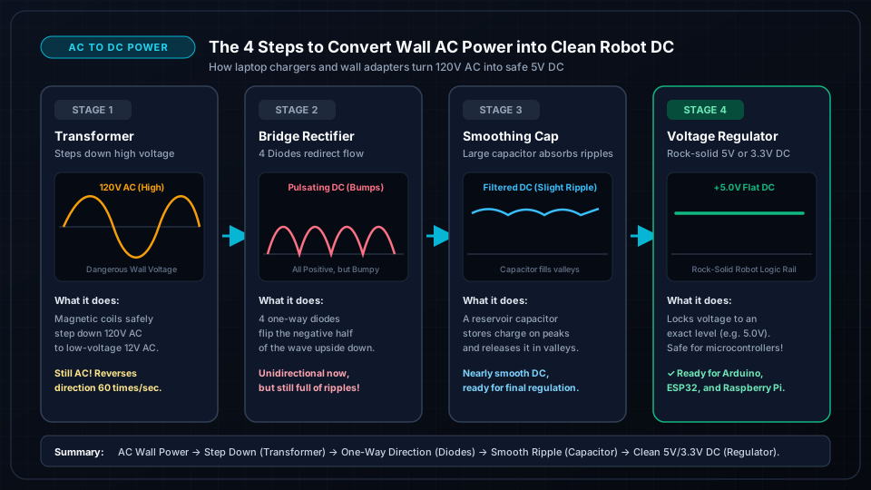
A Full-Wave Bridge Rectifier arranges 4 diodes in a diamond configuration to convert both positive and negative AC half-cycles into pulsating positive DC:
- During the positive half-cycle, diodes D_1 and D_2 conduct.
- During the negative half-cycle, diodes D_3 and D_4 conduct, steering current into the load in the exact same direction.
- A reservoir capacitor placed across the output smooths the remaining ripples into steady DC.
Frequently Asked Questions
What is a Flyback Diode and why is it essential for motors and relays?
DC motors and relay coils are inductors. When current is suddenly switched off, the collapsing magnetic field creates a reverse high-voltage spike (Back-EMF) often exceeding 100V. A flyback diode placed in reverse parallel across the coil gives this spike a safe loop to dissipate, protecting driving transistors from destruction.
What makes a Zener Diode different from a regular diode?
A regular diode blocks reverse current until it fails. A Zener diode is engineered to conduct backwards at a precise, stable breakdown voltage (e.g. 3.3V, 5.1V, 12V), making it perfect for simple voltage references and overvoltage protection.