Key Engineering Takeaways
- •A schematic diagram represents electrical connections logically, not physical component locations on a board.
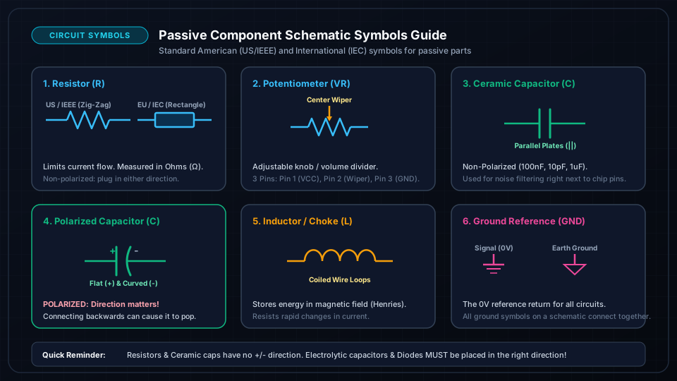
- •A black dot at a wire intersection indicates an electrical junction; crossed wires WITHOUT a dot do NOT connect.
- •American schematics use a zig-zag line for resistors, while European/IEC schematics use a rectangular box.
- •Polarized symbols (electrolytic capacitors, diodes, LEDs, transistors) have distinct markings that dictate physical orientation.
- •Net labels (e.g., "SDA", "TX1", "VCC") allow logical connections across schematics without drawing long cluttered wire lines.
Prerequisites
- • Basic component familiarity (Resistors, LEDs, Batteries)
Required Hardware / Tools
- • Sample Schematic Printout
- • Multimeter
- • Breadboard and components for practice circuit
Why Schematics Matter: Logical vs Physical Layout
A **Circuit Schematic** is the universal blueprint of electrical engineering. It uses standardized symbols to describe how components connect logically, completely independent of their physical shapes or mechanical packaging.
### Logical vs Physical:
- A physical photo or pictorial diagram shows component shapes and wire colors, which becomes confusing for complex circuits.
- A schematic organizes current flow logically from **Left to Right** (Inputs on the Left to Outputs on the Right) and voltage from **Top to Bottom** (Positive Voltage Rails at the Top to Ground at the Bottom).

Passive Component Symbols (Resistors, Capacitors, Inductors)
Passive components cannot amplify signals on their own, but they shape voltage, filter noise, and regulate current flow.
### 1. Resistors:
- **US / IEEE Standard**: A classic zig-zag line.
- **IEC / European Standard**: A simple rectangular box.
- **Potentiometer (Adjustable Resistor)**: A resistor symbol with a diagonal or center arrow pointing to it, representing the sliding wiper pin.
### 2. Capacitors:
- **Non-Polarized (Ceramic & Film)**: Two straight parallel plates (||). They can be inserted into a breadboard in either direction.
- **Polarized (Electrolytic)**: One flat plate (positive +) and one curved plate (negative -). Direction matters: connecting backwards can cause them to burst!
### 3. Inductors & Transformers:
- **Inductor (Choke)**: A series of coiled wire loops or curved bumps representing a wound wire coil.
- **Transformer**: Two inductor coils sitting opposite each other, separated by two parallel lines representing the magnetic core.
Semiconductor Symbols (Diodes, Transistors, ICs, Op-Amps)
Active components control the flow of electricity using semiconductor physics to amplify, switch, or compute.
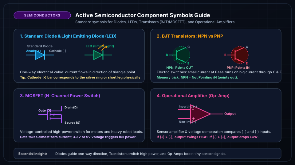
### 1. Diodes & LEDs:
- **Standard Diode**: A triangle pointing into a vertical line. Think of the triangle as an arrow showing current direction: current flows from **Anode (+)** to **Cathode (-)**.
- **LED (Light Emitting Diode)**: A diode symbol with two small arrows pointing outward into space, indicating that it radiates visible light.
- **Zener Diode**: The vertical cathode bar has bent Z-shaped wings, showing it can safely conduct backwards at a specific breakdown voltage.
### 2. Transistors (Switches & Amplifiers):
- **NPN BJT**: The arrow on the emitter points **OUT** (a handy memory trick: **N**ot **P**ointing i**N**).
- **PNP BJT**: The arrow on the emitter points **IN** (**P**ointing i**N** **P**roudly).
- **N-Channel MOSFET**: Has three terminals labeled Gate (G), Drain (D), and Source (S). Gate is separated by a tiny insulated gap—voltage at the Gate controls heavy current flowing from Drain to Source.
### 3. Operational Amplifiers (Op-Amps):
- A large triangle with two inputs on the flat side (Inverting marked with '-' and Non-Inverting marked with '+') and one output pin at the pointed tip.
Wires, Junction Dots & Net Labels: Connected vs Crossing
Understanding how lines on a schematic represent actual physical connections:
1. **Junction Dot (●)**: When two crossing or intersecting lines have a solid dot at their connection point, they are **electrically joined together**. Think of it as a soldered T-junction or crossroad: electric current flows freely between all branches. On your breadboard, you plug these wires into the same row.
2. **Crossing Lines (No Dot)**: When two lines cross like a "+" with **no dot** (or with a small curved bridge arch), they are **isolated wires passing over each other** with zero electrical contact—just like two highway overpasses. They are completely separate circuits! On your breadboard, keep them in separate rows.
3. **Net Labels (Named Wires)**: To keep diagrams clean and prevent a giant spaghetti-tangle of crisscrossing lines, modern circuit design tools (like KiCad, Altium, and EasyEDA) use names. Any two wire stubs that share the exact same label (like `VCC`, `GND`, `I2C_SDA`, or `MOTOR_PWM`) are secretly connected together in the background.
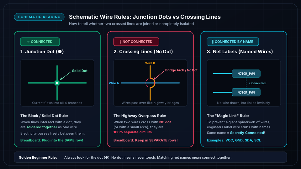
The Golden Junction RuleAlways look for the solid dot (●). If two crossing wires lack a dot, NEVER connect them together on your breadboard!
Step-by-Step: Translating a Schematic to a Breadboard
Follow this proven 5-step hardware assembly workflow:
1. **Place ICs First**: Insert microcontrollers, op-amps, and chips across the center breadboard trough.
2. **Wire Power & Ground**: Connect chip VCC and GND pins directly to the breadboard power rails (+ and -). Add 100nF decoupling capacitors right next to each chip power pin.
3. **Connect Passive Components**: Connect resistors, capacitors, and pull-up resistors to their designated chip pins.
4. **Connect I/O Peripherals**: Wire buttons, LEDs, potentiometers, and sensor modules.
5. **Continuity Verification**: Before applying battery power, use your digital multimeter in continuity (beep) mode to verify that VCC and GND are not shorted together.

Frequently Asked Questions
What do reference designators like R1, C2, and Q3 mean?
Reference designators uniquely identify each component on the schematic and PCB: R = Resistor, C = Capacitor, L = Inductor, D = Diode, Q = Transistor, U or IC = Integrated Circuit, J = Connector, SW = Switch.
What is the difference between Chassis Ground, Earth Ground, and Signal Ground?
Signal Ground (downward triangle or horizontal bars) is the 0V reference for circuit signals. Chassis Ground (rake symbol) connects to the metal enclosure for safety and shielding. Earth Ground connects physically to a copper rod driven into the earth for mains safety.
Tags:#Schematics#Circuit Symbols#Electronics Design#EDA#KiCad#Schematic Reading